E Beam Wafer Inspection

E Beam Inspection Makes Inroads

Hmi Ep5 Metrology Inspection Systems
Electron Beam Semiconductor Wafer Pattern Verification System Product Information Tasmit Inc
Https Www Mdpi Com 2079 9292 6 4 87 Pdf Vor
Kla Introduces Breakthrough Electron Beam Defect Inspection System Semiconductor Digest

E Beam Wafer Inspection System Market Trends Growth Opportunities And Global Outlook 2020 To 2026 Galus Australis

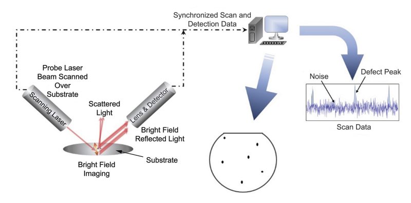
E beam or electron beam wafer inspection system refers to a part of semiconductor fab equipment used for the wafer manufacturing process.
E beam wafer inspection.

Automated Inspection Machine Edr7xxx Series Kla Tencor Optical For Wafers Defect

Non Invasive Nanolithography Heidelberg Instruments The Power Of Direct Writing In 2020 Covalent Bonding Heidelberg Writing
Semiconductor Inspection
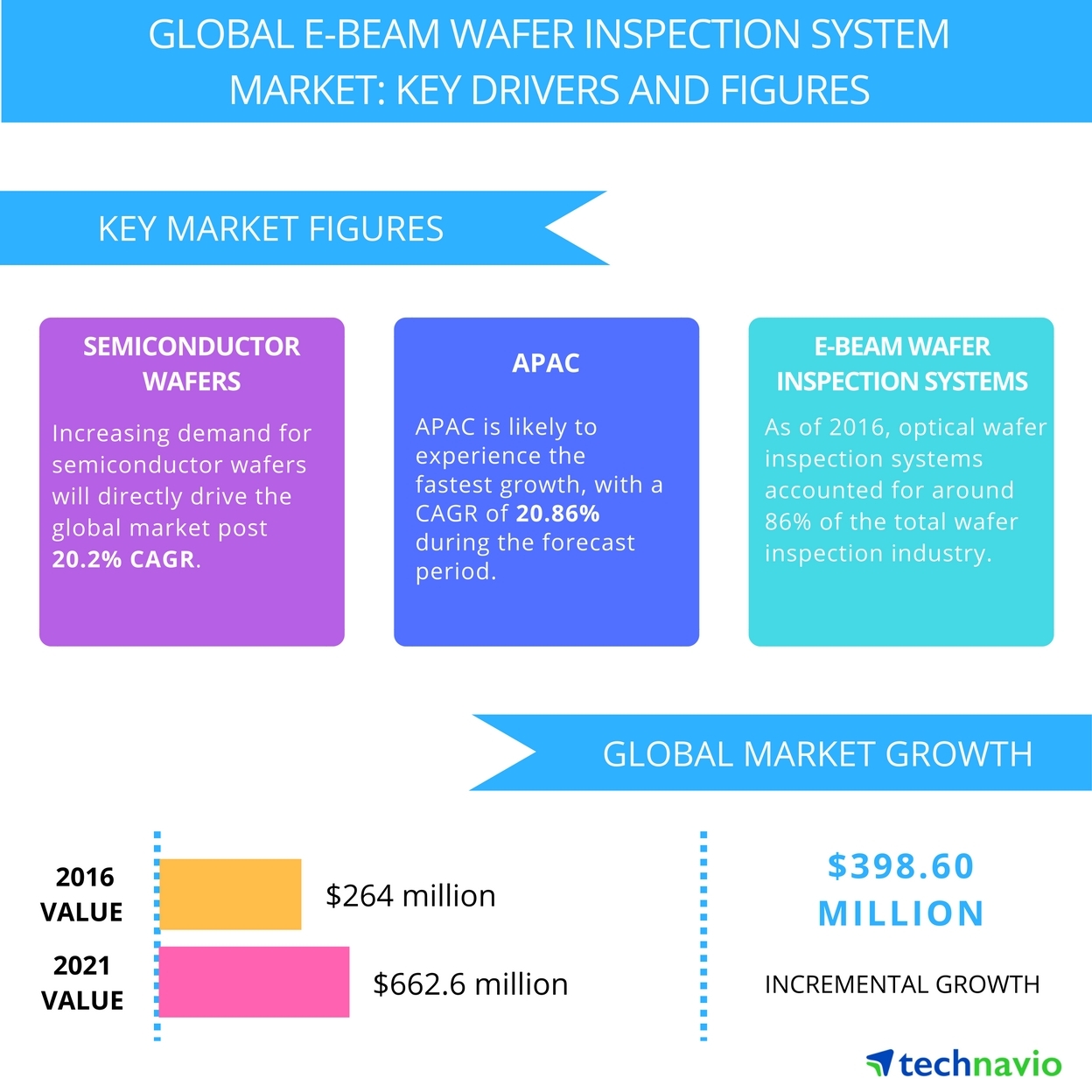
E Beam Wafer Inspection System Market Drivers And Forecast From Technavio Business Wire
Product Information Tasmit Inc

Global E Beam Wafer Inspection System Market 2020 Hermes
Kla Announces New Defect Inspection And Review Portfolio Semiconductor Digest

Global E Beam Wafer Inspection System Market 2015 2019 Youtube

Cause And Effect Diagram Template Luxury Cause Effect Diagrams Lean Six Sigma Training Ursache Und Wirkung
Wafer Inspection System Inspectra Series Optical Semiconductor Wafer Inspection System Product Information Tasmit Inc

Kla Tencor Defect Analysis On Another Level News
Pdf Smart E Beam For Defect Identification Analysis In The Nanoscale Technology Nodes Technical Perspectives

Hmi Escan 430 Metrology Inspection Systems
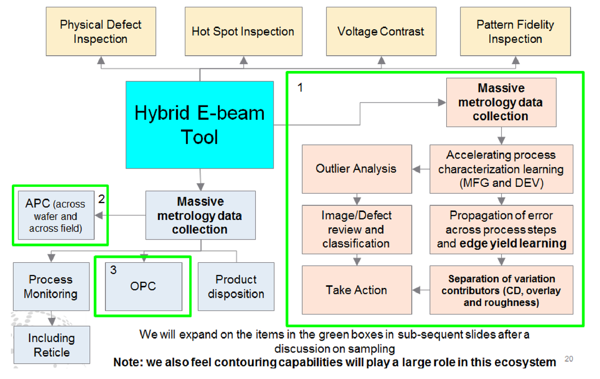
In Line E Beam Metrology And Defect Inspection Industry Reflections Hybrid E Beam Opportunities Recommendations And Predictions

Wafer Inspection Stages Nanomotion
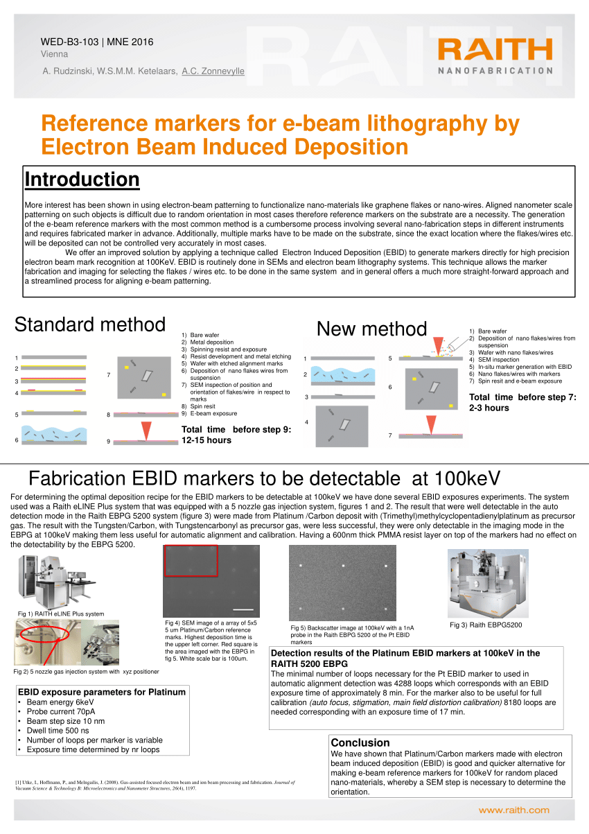
Pdf Reference Markers For E Beam Lithography By Electron Beam Induced Deposition
Kla Tencor Es31 E Beam Wafer Inspection System

Using E Beam Inspection And Overlay As Tool For Identifying Process Weaknesses In Semiconductor Processing

Nsf14 H Zf12 China Factory From China If You Are Interested Pls Tell Me Your Email I Can Send Details To Your Email Acoustic Wave Crystal Growth Surface

E Beam Wafer Inspection System Market By Technology Market Research Report Issuu

High Accuracy High Speed And Smart Metrology In The Euv Era

Kla Tencor Es30 E Beam Wafer Inspection System Go Dove
Electronics Free Full Text Smart E Beam For Defect Identification Amp Analysis In The Nanoscale Technology Nodes Technical Perspectives
Global E Beam Wafer Inspection System Industry
Source : pinterest.com
